Do you know how an optical transceiver maintains stable transmission? Today, we will introduce the weapon for maintaining stable transmission of optical modules - the gold finger.
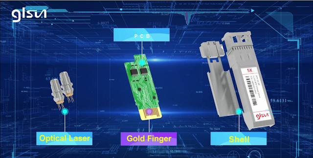
An optical transceiver typically consists of optical devices, a functional circuit board (PCB), a shell, and other parts. And, the gold finger is a critical part of signal transmission. The "gold finger" of an optical transceiver refers to the gold-plated conductive contacts on the PCB board, which are mainly used to connect to other devices. The gold finger is responsible for transmitting signals and power, and ensuring the normal operation of the optical transceiver. Additionally, the thickness of the gold plating on the gold finger directly affects the transmission quality of the optical module, such as issues like current and voltage fluctuations or abnormal temperature increases.
1. Electroplating Nickel Gold
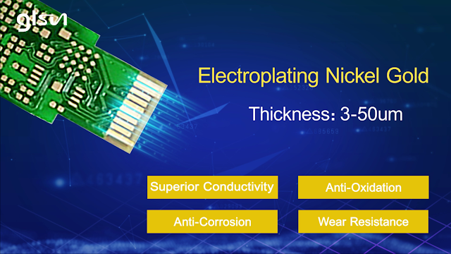
Gold plating is a surface treatment process for PCBs. With a thickness ranging from 3-50 μm, it has excellent conductivity, oxidation resistance, and wear resistance, making it widely used in gold finger PCBs that require repeated plugging and unplugging. Due to the high cost of gold plating, it is only applied to gold finger and other localized gold plating treatment.
Advantages of Electroplating Nickel Gold
- Superior Conductivity
- Anti-Oxidation
- Anti-Corrosion
- Reduce Contact Resistance
- Wear Resistance
2. Sinking Gold
- Superior Conductivity
- Anti-Oxidation
- Anti-Corrosion
- Reduce Contact Resistance
- Wear Resistance


没有评论:
发表评论